Circuit Board Layout of Electronic Systems
Engineering Institute of Technology Australia
Module 16: Practical Shielding EMC/EMI, Noise Reduction, Earthing & Circuit Board Layout of Electronic Systems
SAVE TOP GRADE USING CIRCUIT BOARD LAYOUT OF ELECTRONIC SYSTEMS ASSIGNMENT HELP SERVICE OF EXPERTSMINDS.COM
Question1 Interference is present in a signal cable between a PLC and a temperature sensor which is running next to a power cable in the tray.
a) List and briefly describe the different types of noise coupling paths possible.
b) List any 2 ways of minimizing the coupling issues?
Noise coupling or interference in a signal cable can occur in four possible ways, Common Impedance coupling, Inductive Coupling, Radiative Coupling, and Capacitive coupling.
1) Common Impedance Noise: Common Impedance Noise might occur in the circuit due to presence of impedance (can inductive, capacitive, or reactive) in the common return path of two circuits. This may result in the error of voltage measurement depending on the value of current in the circuit and amount of impedance.
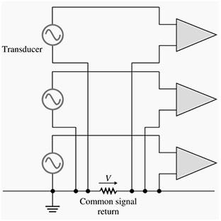
Fig. 1: Common Impedance Noise coupling
2) Inductive Coupling: These noises are produced by mutual induction between two nearby circuits. A time varying magnetic field is produced by the noise circuit (due to flow current) causes voltage induced in the signal circuit as given by the formula.
Vn = 2p fBACos∅ , where symbols have their usual meaning.
A lumped equivalent circuit can be used to explain the same where this coupling is represented by a mutual inductance placed between them.
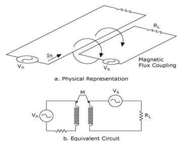
Fig. 2: Inductive Coupling
DO YOU WANT TO EXCEL IN CIRCUIT BOARD LAYOUT OF ELECTRONIC SYSTEMS ASSIGNMENT - ORDER AT EXPERTSMINDS!
3) Capacitive Coupling: It is caused due to disturbance due to electric field from noise circuit to signal circuit. This transfer of energy due to electric field is equivalent to a capacitance placed between them, which form the basis of conversion of the scenario into a lumped equivalent circuit as shown in the figure.
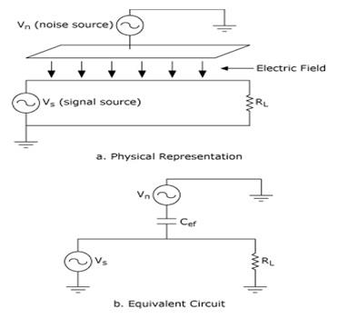
Fig. 3: Capacitive coupling
4) Radiative Coupling:
This type of coupling occurs due to radiation from TV or Broadcast radio sources or any other communication channel.
Two ways to minimize noise coupling are:
i) By using different return paths for signals
ii) By using twisted cable in the circuit (Cao et al., 2018)
Question2 The fundamental to an understanding of EMC are the concepts of differential mode, common mode and antenna mode radiated field coupling.
List any 5 differences between differential mode and common mode coupling.
Answer2 In differential mode coupling, coupling occurs in two lines of a closed loop where current flows in opposite direction. However, common mode coupling occurs in two lines in the same direction and phase.
In differential mode coupling, disturbances are weakly coupled because of conductors being placed nearby. In Common mode coupling, current can be induced due to magnetic fields.
In differential mode coupling, the current is generally larger whereas in current mode coupling the current is very small.
In differential mode coupling, the area of the loop is very small compared to common code.
The solution of differential mode coupling is connection of impedance series in with the high side along with a shunt capacitor across the line. However, common mode coupling can be solved using a common-mode choke (Chen, Chen, Chiu, & Yeh, 2015)
Question3 Describe in at least 4 sentences how an electronic circuit can create an electromagnetic (EM) wave.
Answer3 We know all electronic components work on electric current. A time varying electric field generates a time varying magnetic field and vice versa. Now, an electronic circuit has got both electric (capacitors) and magnetic (inductors) components. So, when an alternating electric current (which varies with time) is applied in an electronic circuit, it produces time varying electric and magnetic fields. These interactions between electric and magnetic fields cause the production of an electromagnetic wave.
Question4 List any 2 primary sources of transients and spikes.
Answer4 Two sources of transients and spikes are:
1. Arcing faults
2. Contactor, breaker or relay operations.
Question5 Describe 2 methods to prevent CM (common mode) to DM (differential mode) conversion in circuits that carry high-frequency signals (such as wideband data or video) or which could be susceptible to RF.
DON'T MISS YOUR CHANCE TO EXCEL IN CIRCUIT BOARD LAYOUT OF ELECTRONIC SYSTEMS ASSIGNMENT!
Answer5 Two methods are as follows:
1. If an EMI filter includes both CM & DM then DM should have less than 30 MHz where as it can increase due to magnetic influx that can be controlled by mode choke. The CM should be 30-100MHz. Then both filters would require limited EMI for entire frequency.
2. As most circuit carry high frequency thus it can be susceptible to RF. The best possible way to prevent conversion from CM – DM is reducing the unwanted impedance. This would equalize the frequency as much as possible.
Question6 Explain the difference between EMI and EMC.
Answer6 EMI stands for Electromagnetic Interferences whereas EMC stands for Electromagnetic Compatibility. Electromagnetic interference refers to any disturbance, which is occurring in the circuit due to external sources. On the other hand, Electromagnetic Compatibility refers to devices ability to withstand any kind of electromagnetic interference( Cole, Linnebur, Preston, & Schofield, 2018).
Question7 A micro-processor circuit with a clock frequency of 10MHz has been mounted in a metal enclosure. There are, however, some concerns about emissions leaking from the enclosure with the screws screw separation distance x. Close to the micro-processor circuit is a 100MHz receiver circuit which receives noisy signals. The receiver is sensitive at 10 times the clock frequency of the micro-processor circuit and one would have assumed that the 10th harmonic of a square wave would be significantly reduced.
a) You first suspect that (as the other people thought) some RF might be leaking from the lid. You open the lid but the noise at the receiver does not increase a lot. In fact, taking the lid away does not make a big difference. Discuss what might be the problem and if it is possible to emit at 100MHz. Also recommend what the distance x between the screws should be.
b) You are still confronted with a heat problem and need to make holes in the box for forced air cooling. What is the maximum whole size allowable if the people using the receiver inform you that 20dB attenuation should be enough?
c) If the hole size in 5.2 is not adequate for cooling, what can be implemented to increase the hole size without compromising the 20dB attenuation.
Answer7 a) If RF is not the problem then there might be some interference from other external sources.
The distance x should be 2.1 mm.
b) Maximum whole size should be 3mm.
c) Yes, it is adequate for cooling. However, further whole size can be increased if necessary.
Question8 Although lightning and ESD are both pulsed noise, they differ in their treatment and threats. Describe why they are two distinct threats (list at least 3 differences).
Answer8 ESD or Electrostatic discharge is a phenomenon in which there is a sudden electricity flow between two charged objects whereas lightning are those ESDs, which occur naturally.
ESD are caused by the method of electrostatic induction (when a charged body is placed near an uncharged conductor, it induces an electric charge in it). Lightning is caused due to discharges occurring due to clouds.
ESD causes very high voltage spikes in the system thus causing damage and lightning can cause voltage difference between earth and neutral wires, which should ideally be zero ( Curran et al., 2016).
HIRE TUTOR OF EXPERTSMINDS.COM FOR PERFECTLY WRITTEN CIRCUIT BOARD LAYOUT OF ELECTRONIC SYSTEMS ASSIGNMENT SOLUTIONS!
Question9 With diagrams/figures explain the relationship between spectrum usage and created interference.
Note – This question is mandatory. It should be answered and students are expected to get this question completely right to be assessed as competent with a score for this module.
Answer9 There is a huge difference between the spectrums, which is used in day-to-day life in various devices through FM and TV broadcast, or long, medium or short- wave radios or mobile phones and the interference created by us.
Interferences created are far different from spectrum usage. The range is usually above 9 kHz. The two given figures quite appropriately explain the difference.
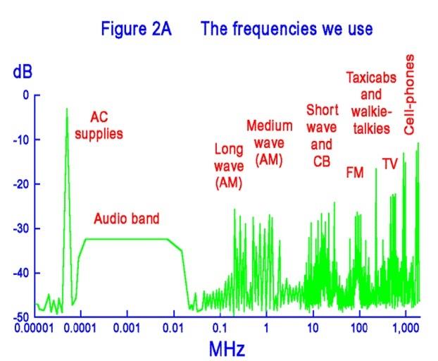
Fig. 4: Spectrum usage
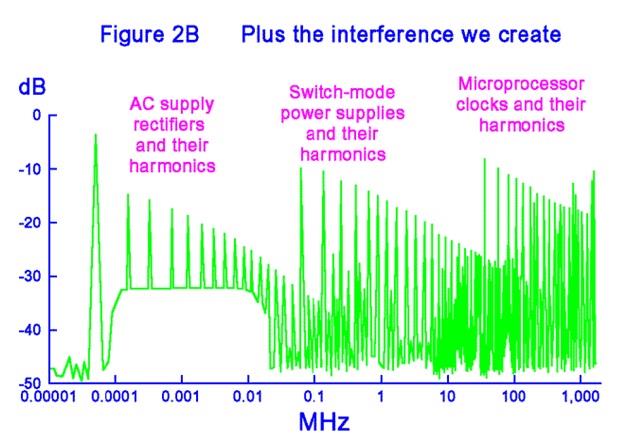
Fig. 5: Interferences created
Question10 With a diagram describe the representation of EMI.
WORK TOGETHER WITH EXPERTSMINDS TUTOR TO ACHIEVE SUCCESS IN CIRCUIT BOARD LAYOUT OF ELECTRONIC SYSTEMS ASSIGNMENT!
Answer10 EMI stands for Electromagnetic Interferences. Electromagnetic interferences refer to noises or disturbances caused in the circuit, which causes errors in measurement. It can happen in many possible manners such conductive interference (caused due to finite impedances in the wire), capacitive interference (caused due to electrical disturbances), inductive interferences (caused due to magnetic disturbances) and radiative interferences (caused due to radiation from various sources).
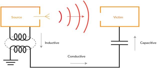
Fig. 6: Various types of interferences
Question11 Provide answers for the following:
a) What is the difference between Earthing and Grounding in the context of EMC?
b) What is the primary EMC function of a ground system.
Answer11 a) Earthing is the process of connecting dead part of the wire, i.e., the part which does not carry, to the ground. On the other hand, grounding is the process of connecting current carrying part to the ground.
b) Basic EMC function of a ground system is to protect the electrical equipments from damage.
Question12 Discuss 3 ways that grounding systems for a circuit reference can be configured.
Answer12 The three configurations of grounding are single point grounding, multi point grounding and hybrid grounding.
Single point grounding: As the very terminology suggests, single point grounding involves grounding of all circuit elements at a single point, for this all the circuit elements connected to a single wire, and that wire is grounded at a point.
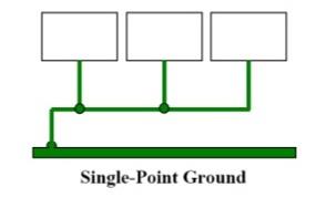
Fig. 7: Single point Grounding
Multi-point grounding: Unlike single point grounding, here each circuit elements grounded separately at many points on the ground.
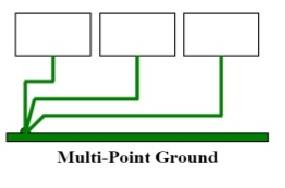
Fig. 8: Multi-Point Grounding
Hybrid Grounding: In this system, each circuit element is connected to the ground accompanied by a reactive element like capacitor or inductor.
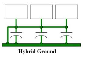
Fig. 9: Hybrid Ground
Question13 The major source of radiation in digital circuits is the processor clock(s) and its harmonics. All the energy in these signals is accumulated at a few specific frequencies, with the result that the clock signal levels are 10 to 20 dB higher than the rest of the digital circuit radiation.
a) Since the commercial radiated emissions standards do not distinguish between narrowband and broadband how can you reduce the narrowband emissions?
b) List the high frequency broadband sources.
c) If circuit constraints allow, list the methods that can be used to slow down clock rates in order to minimize harmonic generation.
d) How can we decrease the level, measured in a constant 120 kHz bandwidth falls, by between 10 to 20 dB without any extra effort made in layouts and without slowing the clock rise times?
Answer13 a) The narrow emission can be restricted as follows:
1) By using proper layout
2) By doing proper grounding
3) The clock lines should be buffered
b) The list of high frequency broadband sources is as follows:
1) Nuclear Electromagnetic Pulse
2) Ultra Wide Band
3) HPM High Power Magnetic radio transmitter (used in military communications) and weapons
c) There are three ways of reducing the rates of clocks:
1) By putting impedance in series, We can increase the series impedance of the driver output at its harmonic frequency, for this, we must put a small ferrite impeder in series with output.
2) By putting capacitor in parallel, This method is generally undesirable as it increases capacitive load on the driver so its effect can rather make the emission worse instead of improving it.
3) By using low performance buffer.
d) Level of constant can be decreased by Spread Spectra Clock Generation technique. In this particular technique, the frequency of the clock modulated at 0.5-2%. The waveform selected in this technique is basically is known as even spectra spreading. This technique helps in providing a wider spectral energy. By using it, the Bandwidth falls from constant 120kHz to 10-20 Db. Patented by Lexmark 1996.
Question14 Why is it difficult or almost impossible to shield against magnetic fields at low frequencies (at least 4 points required)?
Answer10 1. Low frequency magnetic fields are usually generated from sources like motor, power supplies, transformers, and switches.
2. These low frequency magnetic fields generally cause huge EMI challenges because of the critical precision or accuracy of the circuit.
3. Generally, materials with high magnetic permeability can be used to prevent this problem.
4. These materials redirect magnetic noises away from the device thus protecting the magnetic field (Fang et al., 2016).
Question15 Generally, analog circuits are not as susceptible to transient upset as digital ones, but may be more susceptible to demodulation of RF energy. Describe at least 4 points on how to restrict the operating bandwidth to the minimum acceptable level in order to reduce the level of interfering signal.
Answer15 The four ways of restricting operating bandwidth to the minimum acceptable level are as follows:
1. WORPsync helps in reducing the bandwidth level significantly in self-interface level. The system acts as a tool for radio signal transmission it also helps in increasing
2. DCS also known as Dynamic Chanel Selection regarded as a tool. It ensures steady reliable quality of link by reducing the interfering link within a signal.
3. ATPC also known as Automatic Transmit Power Control, it is regarded as a feature that helps point to multipoint and P to P that is point to point. It dynamically corrects the transmitting power to the optimal condition.
4. Proper Chanel Spacing helps in creating proper frequency between two points thus by eliminating the interfering signals (Halligan, 2107).
Question16 List any 3 advantages and 1 disadvantage of surface mount devices (SMDs).
Answer16 Advantages: Some of the advantages of SMDs are:
1) Reduced component size, which enables it to fit in fewer boards.
2) These are more reliable and less prone to failures, so it can withstand any kind of vibration or shaking.
3) Lower costs.
Disadvantage: One of the major disadvantages of SMD is that its solder joints are small in size, which reduces its reliability (Halligan, 2107).
Question17 List and briefly describe the 4 basic types of Surge Protection devices (SPDs).
Note – This question is mandatory. It should be answered and students are expected to get this question completely right to be assessed as competent with a score for this module.
Answer17 Four types of surge protector devices are described as follows:
Type 1-surge protectors acts as first layer of protection against lightning or other sources. It is of outdoor use.
Type 2-surge protectors, which is also known as, branch surge panels protects branch circuits or entrance service entrance from various kinds of surges. It is mainly of industrial, residential, or commercial use.
Type 3-surge protectors or power strips electronic household appliances (like TV, PC, etc.) from low-level surges, which could damage these devices. Therefore, they are the last line of household defense.
Type 4-surge protectors also known as surge protection modules offer a bit different type of protection than Type 3. These can protect industrial applications as well as commercial and industrial equipment cabinets.
Question18 List the principles used in PCB shielding.
Answer18 Principles for PCB shielding are as follows:
• For both high and low frequency for E-field application any metal would do, but higher conductive metal should be selected
• For Low frequency in the H-field a permeable metal or casing should be selected
• With a circuit of 0V plane on board shield should be used normally in conjunction. However, inadequate plane would reduce its effectiveness.
Outer enclosures in partitioning houses are not required to be always shielded. Partitioning into dirty and clean box is also effective. It can be easily done with on board shielding (Huang & Dai, 2017)
ARE YOU LOOKING FOR RELIABLE CIRCUIT BOARD LAYOUT OF ELECTRONIC SYSTEMS ASSIGNMENT HELP SERVICES? EXPERTSMINDS.COM IS RIGHT CHOICE AS YOUR STUDY PARTNER!
Question19 Briefly describe any 4 applications for different type of screened cables.
Answer19 Types of screened cables are as follows:
• Coaxial Cable: It has a copper plated core and a dielectric core insulator covers it. It surrounded by a woven copper shield and finally covered by a plastic sheath, applied in connecting feed lines in radio transmission.
• Ribbon Cable: Also known as Multi wire planar cable or flat twin cable. Such cables are simple insulated wires, running parallel to each other. The cable transmits multiple signal data. Applied internally in multiple electronic peripherals.
• Twisted pair cable: Such cables are color-coded and it consists of multiple copper insulated wires twisted together to form a single cable. The wire ranges from 0.4 to .8mm and numbers of wires vary as well, applied in data networks for both medium and short connections.
• Shielded cable: Consists of single or multiple insulated wires. It is further braided in aluminum Mylar foil or braid shield, used in multiple electronic peripheral for wire protection.
Question20 What are 2 main principles of cable routing?
Answer20 Two main principles of cable routing are as follows:
• Source and target components should have direct connecting in between them
• Return and Send conductors should be routed closely (Kukreja, Xu, Leftik & Srinivasan, 2017).
Question21 List any 2 advantages of using screened connectors.
Answer21 Two advantages for using screened connectors are as follows:
• Such connectors are resistant to the UV, ozone, mechanical abuse and chemical abuse
• It suitable for 12kV-36kV cables (250amp-1250amp)
Question22 List any 3 filter thumb rules for various available conditions for unwanted signals?
Answer22 Three filter thumb rules are as follows:
• Fred Hariss Thumb Rule
• Kaiser’s Thumb Rule (Formula)
• Transient response
Question23 In at least 5 points describe how does the performance of any filter depend on the impedance seen at its terminal?
Answer23 The five points are as follows:
1. If the source of impedance is zero in shunt filters, then the component to its ground can show zero source of impedance. The zero source of impedance is impractical when driving filters due to cut off frequency. When impedance decreases the current source increases its extraction thus by compromising performance.
2. In the case of infinite load impedance, performance compromised, as it is impractical due to requirement of infinitesimal capacitors & infinite value inductors.
3. Passive filters do not work well with low frequencies where as active filters fails to work with high frequencies. The amplifier in active filters is mainly op-amp. Such amplifier gain high frequency in both low and high frequency thus by providing proper performance.
4. Passive filters made up of capacitor, resistor, and inductors. Most of the cases resistors are only required for load gain some circuit has their own resistors which helps such filters to have a massive load gain in impedance. This further helps the performance to increase due to massive amplification of the signals.
5. In case of low frequency if the filter attenuation is set to 1 dB then the Impedance is much greater than 1 kΩ then only the performance would increase in Passive filters.
Question24 Describe any 2 differences between differential and common mode coupling from PCB’s.
Answer24 The differences between DM and CM coupling from PCBs are as follows:
Differential mode Common Mode
In this mode, the current is on one conductor in one direction where as the phase opposition is on second conductor.
Example: RS-485 and USB
In this mode, the current on both the conductors are in the same direction.
It is also known as symmetrical, as the disturbance in this mode is Weakly Coupled due to conductors being nearby.
It is also known as Longitudinal or asymmetrical. In this mode the current is often induced by an external field to create a strong coupling
Question25 Explain in about 4 sentences what the first and foremost step in PCB layout is
Answer25 The first and foremost step in the PCB layout is consideration of the PCB design. Component orientation plays a major role in designing a PCB layout properly. For Example, while setting resistors and LEDs in a PCB it should always be facing same direction. This would make the PCB layout easy to install and manufacture as well. Thus, considering on how to place the components is one of the major tasks before manufacturing a PCB board.
Question26 Commercial surge protection identifies three distinct zones with differing surge exposure categories. List and briefly describe these categories
Answer26
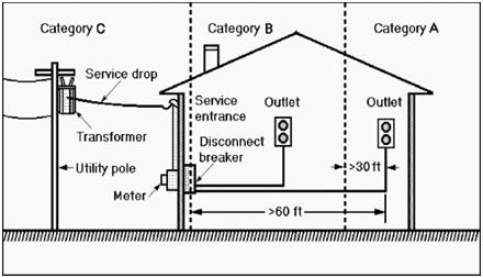
Fig. 10: Three surge protection categories
The three surge protection categories with distinct zones are as follows:
• (Outdoor) Category C: It is the region outside the Commercial Building. It includes External Conductors; it also extends inside the commercial building to its
load centralized circuit breaker or Entrance Disconnect breaker. Example: Power surges due to faulty execution of power generators.
• (Indoors) Category B: It is a zone within the commercial building. The range extends at least 10m (30 ft) from branch circuit to electrical receptacles or outlets. Example: High voltage in any commercial apparatus.
• (Indoors) Category A: It is a zone that is farthest from the commercial disconnect breaker. The Zone that extends from branch circuits to the entire outlets is more than 30ft in Category B and more than 60 ft from the Service Entrance Disconnect Breaker in category C.
Question27 Describe the principle of using transmission lines on PCB’s.
Answer27 Circuit Design exposed to a variety of occasions is termed as Transmission line. It is one of the many elements. It puts emphasis on the Signal Integrity analysis. This is the reason why many analysts built on this basis. Transmission line considered suitable for the electrical power or Electrical Signal Transmission in between two or more terminals.
Attain our Engineering Institute of Technology Assignment Help Services for its related academics programs and major units such as:-
- Basic Electrical Engineering Assignment Help
- Troubleshooting Electronic Components and Circuits Assignment Help
- Technical and Specification Writing Assignment Help
- Shielding, EMC/EMI, Noise Reduction and Grounding/Earthing Assignment Help
- Fundamentals of Professional Engineering Assignment Help
- Embedded Microcontrollers Assignment Help
- Biomedical Modelling and Simulation Assignment Help